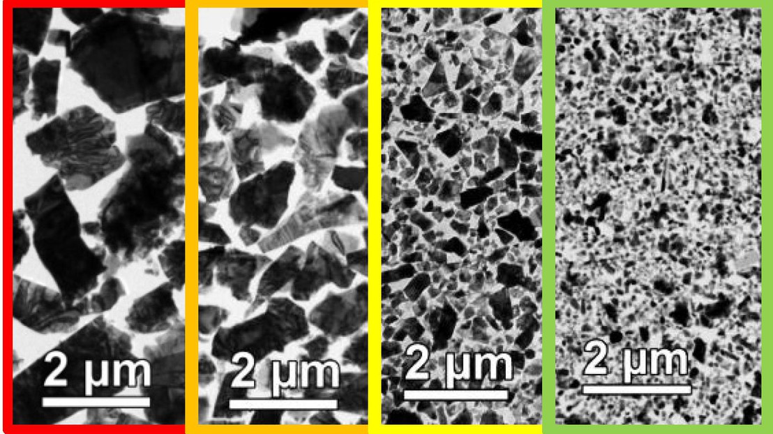
A novel nanoflake size sorting technique for 2D "layered" materials

© K. Sivula /EPFL 2017
Dr. Xiaoyun Yu's report on the effect of flake size on 2D nanoflake WSe2 photocathodes introduces a new separation technique and employs a photogenerated carrier transport model to gain new insights into the performance of this material toward solar energy conversion.
Understanding and optimizing the effects of edge states and nanoflake dimensions on the photon harvesting efficiency in ultrathin transition-metal dichalcogenide (TMD) semiconductor photoelectrodes is critical to assessing their practical viability for solar energy conversion. In a paper publised in Chem. Mater. Yu and Sivula team up to demonstrate a novel filtration-based separation approach to systematically vary the TMD nanoflake dimensions and edge density of solution-processed large-area multiflake WSe2photocathodes. Photoelectrochemical measurements in both aqueous electrolyte (for water reduction) and a sacrificial redox system, together with a continuum-based charge transport model, reveal the role of the edge sites and the effects of the flake size on the light harvesting, charge transport, and recombination. A selective passivation technique using atomic layer deposition is developed to address detrimental recombination at flake edges. Edge-passivated WSe2 films prepared with the smallest flakes (∼150 nm width, 9 nm thickness) demonstrate an internal quantum yield of 60% (similar to bulk single-crystal results). An optimized (1 sun) photocurrent density of 2.64 mA cm–2 is achieved with 18-nm-thick flakes (700 nm width) despite transmitting ∼80% of the accessible photons. Overall, our results represent a new benchmark in the performance of solution-processed TMDs and suggest routes for their development into large-area low-cost solar energy conversion devices.